| CPC H01L 22/34 (2013.01) [G09G 3/006 (2013.01); G09G 3/3233 (2013.01); H01L 27/1237 (2013.01); H01L 27/1248 (2013.01); H01L 27/1255 (2013.01); H01L 29/786 (2013.01); G09G 2300/0413 (2013.01); G09G 2300/0426 (2013.01); G09G 2310/0232 (2013.01); H10K 59/12 (2023.02); H10K 59/1201 (2023.02); H10K 59/88 (2023.02)] | 7 Claims |

|
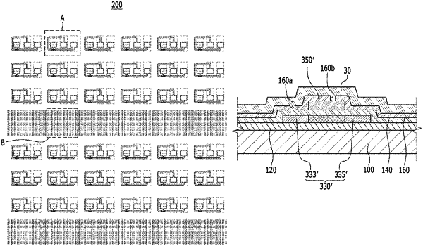
1. A display device comprising:
a substrate including a display area and a non-display area disposed adjacent to the display area;
a pixel disposed in the display area and including a display thin film transistor (TFT), wherein the display TFT includes a display semiconductor layer;
a first dummy circuit disposed in the non-display area,
wherein the first dummy circuit includes a first dummy semiconductor layer and a first dummy gate electrode overlapping at least a portion of the first dummy semiconductor layer in the depth dimension of the display device, and
wherein the display semiconductor layer and the first dummy semiconductor layer have substantially the same shape; and
at least one test element group (TEG) disposed in the non-display area and including a test TFT and at least one test pad electrically connected to the test TFT, wherein the test TFT includes the first dummy semiconductor layer, and
wherein the test pad is connected to the first dummy semiconductor layer of the first dummy circuit,
wherein the first dummy semiconductor layer of the first dummy circuit and the first dummy gate electrode are connected to each other through the test pad,
wherein the test TFT further comprises an interlayer insulating layer disposed on the first dummy semiconductor layer and the first dummy gate electrode, wherein the test pad penetrates a portion of the interlayer insulating layer that overlaps an upper surface of the first dummy gate electrode,
wherein the penetrated portion, of the interlayer insulating layer, vertically overlaps the upper surface of the first dummy gate electrode,
wherein the test pad completely covers the upper surface of the first dummy gate electrode.
|