| CPC H01L 21/823431 (2013.01) [H01L 21/823412 (2013.01); H01L 21/823481 (2013.01); H01L 21/823821 (2013.01); H01L 29/0673 (2013.01); H01L 29/42392 (2013.01); H01L 29/66742 (2013.01); H01L 29/6681 (2013.01); H01L 29/7851 (2013.01); H01L 29/78696 (2013.01)] | 20 Claims |

|
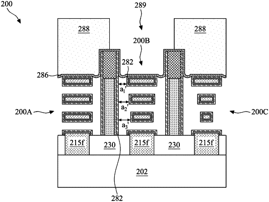
18. A semiconductor structure, comprising:
a dummy fin disposed over an isolation structure;
a stack of channel layers adjacent to the dummy fin, wherein widths of the channel layers of the stack of channel layers increase as they are further away from an underlying substrate;
a first high-k dielectric portion wrapping around a first channel layer of the stack of channel layers;
a second high-k dielectric portion wrapping around a second channel layer of the stack of channel layers, the second channel layer closer to the underlying substrate than the first channel layer; and
a third high-k dielectric portion disposed on sidewalls of the dummy fin;
wherein a first lateral distance between the first high-k dielectric portion and the third high-k dielectric portion is less than a second lateral distance between the second high-k dielectric portion and the third high-k dielectric portion.
|