| CPC H01L 21/76877 (2013.01) [H01L 21/486 (2013.01); H01L 21/76802 (2013.01); H01L 23/5226 (2013.01)] | 12 Claims |
|
1. A forming method of a semiconductor structure, comprising:
providing a base;
forming a bottom dielectric layer on the base;
forming a plurality of hard mask layers extending in a first direction and sequentially arranged in a second direction different from the first direction on the bottom dielectric layer;
etching a part of the bottom dielectric layer located between adjacent hard mask layers in the second direction to form a blocking groove encircled by the adjacent hard mask layers and the bottom dielectric layer;
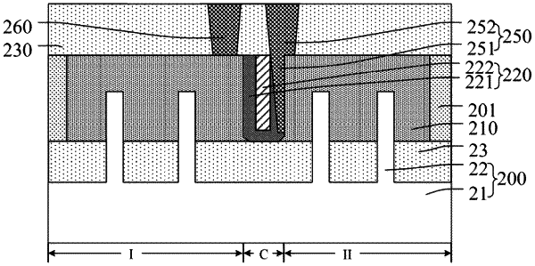
forming a blocking structure filled in the blocking groove;
forming, on the base, a plurality of conductive function layers extending in the first direction and sequentially arranged in the second direction different from the first direction, where the bottom dielectric layer is located between the conductive function layers, and the blocking structure is located in a conductive function layer, the blocking structure segmenting the conductive function layer located on two sides of the blocking structure in the first direction;
etching a part of a thickness of the bottom dielectric layer using the hard mask layers and the blocking structure as masks, to form an interconnection trench in the bottom dielectric layer;
forming a top dielectric layer covering the bottom dielectric layer, the conductive function layers, and the blocking structure;
etching the top dielectric layer located above a junction of the blocking structure and the conductive function layer and a part of the blocking structure located at a side wall of the conductive function layer, to form a via running through the top dielectric layer and exposing a part of a top and a part of a side wall of the conductive function layer; and
filling the via with a via interconnection structure, the via interconnection structure being in contact with the part of the top and the part of the side wall of the conductive function layer.
|