| CPC H01L 21/76846 (2013.01) [H01L 21/76802 (2013.01); H01L 21/7684 (2013.01); H01L 21/76844 (2013.01); H01L 21/76877 (2013.01); H01L 21/76879 (2013.01); H01L 23/5226 (2013.01); H01L 23/5283 (2013.01); H01L 23/53209 (2013.01); H01L 23/53252 (2013.01); H01L 23/53266 (2013.01); H01L 21/3212 (2013.01)] | 20 Claims |
|
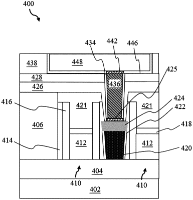
1. A method, comprising:
receiving a workpiece that includes:
a first gate electrode and a second gate electrode,
a first spacer disposed along a sidewall of the first gate electrode,
a first gate dielectric capping layer disposed over top surfaces of the first gate electrode and the first spacer,
a second spacer disposed along a sidewall of the second gate electrode,
a second gate dielectric capping layer disposed over top surfaces of the second gate electrode and the second spacer,
a contact feature disposed between the first spacer and the second spacer along a direction,
a self-aligned contact (SAC) dielectric layer disposed over the first gate dielectric capping layer, the second gate dielectric capping layer, and the contact feature, a portion of the SAC dielectric layer extending between the first spacer and the second spacer as well as between the first gate dielectric capping layer and the second gate dielectric capping layer along the direction, wherein the portion of the SAC dielectric layer is in direct contact with a sidewall of the first gate dielectric capping layer and a sidewall of the second gate dielectric capping layer, and
a first dielectric layer over the SAC dielectric layer;
forming a via opening through the first dielectric layer and the portion of the SAC dielectric layer to expose the contact feature, wherein a portion of the via opening is disposed between a sidewall of the first spacer and a sidewall of the second spacer;
after the forming of the via opening, forming a first reset layer over the exposed contact feature;
depositing a first self-assembled monolayer (SAM) layer on the first reset layer;
after the depositing of the first SAM layer, selectively depositing a first barrier layer on surfaces other than surfaces of the first SAM layer;
removing the first SAM layer;
depositing a via metal fill layer in the via opening to couple to the first reset layer;
depositing a second dielectric layer over the via metal fill layer;
forming a trench in the second dielectric layer to expose the via metal fill layer;
after the forming of the trench, forming a second reset layer over the exposed via metal fill layer;
depositing a second SAM layer over the second reset layer;
after the depositing of the second SAM layer, selectively depositing a second barrier layer on surfaces other than surfaces of the second SAM layer;
removing the second SAM layer; and
depositing a trench metal fill layer over the trench.
|