| CPC H01L 21/76846 (2013.01) [H01L 21/0217 (2013.01); H01L 21/02263 (2013.01); H01L 21/31105 (2013.01); H01L 21/76816 (2013.01); H01L 29/7889 (2013.01); H10B 41/20 (2023.02); H10B 41/35 (2023.02)] | 8 Claims |
|
1. A method comprising:
providing a semiconductor substrate;
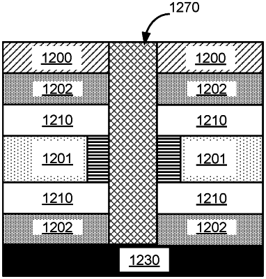
depositing a metal-free multi-layer stack having at least three different materials, at least one of the three different materials being a sacrificial layer;
etching a trench or via in the metal-free multi-layer stack having the at least three different materials;
recessing one of the at least three different materials after etching the trench or via to form a recessed region of the via;
depositing a dielectric or semiconductor material into the trench or via;
etching back the dielectric or semiconductor material in the trench or via to form smooth sidewalls, leaving the dielectric or semiconductor material in the recessed region; and
prior to selectively etching the sacrificial layer, depositing a gate material into the trench or via, and recessing a dielectric material in sidewalls of the trench or via in the metal-free multi-layer stack;
selectively etching the sacrificial layer relative to other materials of the metal-free multi-layer stack to form at least one space between layers of the metal-free multi-layer stack; and
depositing metal in the at least one space to form a metal-containing multi-layer stack having a trench or via etched therein.
|