| CPC H01L 21/743 (2013.01) [H01L 23/535 (2013.01); H01L 29/66795 (2013.01); H01L 21/3081 (2013.01); H01L 21/3086 (2013.01); H01L 21/31111 (2013.01); H01L 21/31155 (2013.01); H01L 21/76224 (2013.01); H01L 29/785 (2013.01); H10B 10/12 (2023.02)] | 20 Claims |
|
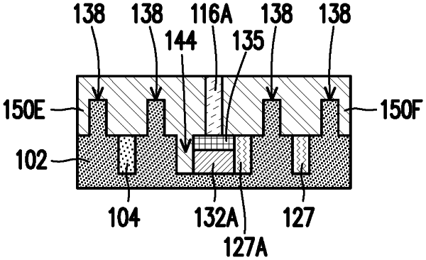
1. A method comprising:
forming a first recess in a semiconductor substrate;
depositing a conductive line within the first recess;
forming a second recess and a third recess along sidewalls of the conductive line;
forming a first fin and a second fin in the semiconductor substrate;
forming a first gate structure over the first fin and in the first recess, the first gate structure contacting a first sidewall of the conductive line;
forming a dielectric material adjacent the conductive line in the second recess; and
forming a second gate structure over the second fin and over the dielectric material.
|