| CPC H01L 21/6833 (2013.01) [H01J 37/32082 (2013.01); H01J 37/32743 (2013.01); H01L 21/3065 (2013.01); H01J 2237/0225 (2013.01); H01J 2237/182 (2013.01)] | 20 Claims |
|
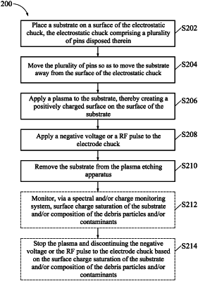
1. A method, comprising:
placing a substrate on a surface of an electrostatic chuck in a wafer processing apparatus, the electrostatic chuck comprising a plurality of pins that protrude therefrom, wherein the wafer processing apparatus includes a process chamber and a source of radio frequency power;
applying radio frequency power from the source of radio frequency power to the substrate to create a positively charged surface on the surface of the substrate;
applying a radio frequency pulse using the source of radio frequency power to the electrostatic chuck to make debris particles and/or contaminants on and/or in proximity of the surface of the electrostatic chuck negatively charged, the debris particles and/or contaminants attaching to the substrate; and
removing the substrate from the wafer processing apparatus thereby removing the debris particles and/or contaminants from the wafer processing apparatus.
|