| CPC H01L 21/68 (2013.01) [H01L 21/6833 (2013.01); H01L 21/6835 (2013.01); H01L 25/0753 (2013.01); H01L 33/007 (2013.01); H01L 33/0075 (2013.01); H01L 33/0093 (2020.05); H01L 2221/68354 (2013.01); H01L 2221/68368 (2013.01)] | 6 Claims |
|
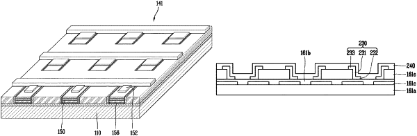
1. An assembly board for positioning semiconductor light emitting diodes at preset positions for manufacturing a display device, the assembly board comprising:
a base portion;
a plurality of assembly electrodes disposed on the base portion;
a dielectric layer on the base portion to cover the assembly electrodes;
a plurality of barrier ribs disposed on the dielectric layer and configured to define a plurality of grooves for guiding the semiconductor light emitting diodes to seating surfaces of the preset positions;
a metal shielding layer at each seating surface formed on the dielectric layer; and
an insulating layer formed to cover the metal shielding layer,
wherein the metal shielding layer overlaps a portion of a corresponding seating surface such that an electric field formed on the portion of the corresponding seating surface is shielded,
wherein the metal shielding layer is formed to overlap with edges of the corresponding seating surface, and
wherein the metal shielding layer includes:
a first region disposed between a corresponding barrier rib and the dielectric layer; and
a second region extending from the first region to overlap the corresponding seating surface.
|