| CPC H01L 21/67167 (2013.01) [B65G 47/90 (2013.01); H01L 21/67196 (2013.01); H01L 21/67126 (2013.01); H01L 21/67706 (2013.01); H01L 21/68707 (2013.01)] | 20 Claims |
|
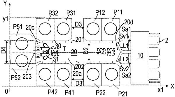
1. A semiconductor processing system, comprising: an elongated transfer chamber including a middle portion, a first end portion and a second end portion, the first end portion and the second end portion being respectively provided at two ends of the middle portion, wherein a first sidewall and a second sidewall of the middle portion are parallel to each other, and wherein the first sidewall and the second sidewall extend in mutually distant directions to form an extended space, resulting in increase of spacing between the first sidewall and the second sidewall at the second end portion;
wherein two lateral semiconductor processing modules comprising a first and a third lateral semiconductor processing modules are provided on the first sidewall and two lateral semiconductor processing modules comprising a second and a fourth lateral semiconductor processing modules are provided on the second sidewall of the middle portion, each lateral semiconductor processing module including two process chambers having predetermined gap between the two processing chambers, the process chambers in each lateral semiconductor processing module being attached, via their respective air-tight valves, to the first or second sidewall of the middle portion of the transfer chamber;
wherein the first end portion of the transfer chamber is communicated to atmospheric environment via a load lock; and
wherein the second end portion of the transfer chamber is attached with one end portion semiconductor processing module, the end portion semiconductor processing module including two process chambers, the two process chambers of the end portion semiconductor processing module being respectively connected to an end face of the second end portion via an air-tight valve;
wherein a first gap space larger than the predetermined gap and larger than 500 mm is provided between the first and the third lateral semiconductor processing modules along the elongate direction of the transfer chamber, the first gap space allowing for access to maintain the process chambers adjacent to the first gap space in the first and third lateral semiconductor processing modules; and
wherein a second gap space larger than the predetermined gap and larger than 500 mm is provided between the second and the fourth lateral semiconductor processing modules along the elongate direction of the transfer chamber, the second gap space allowing for access to maintain the process chambers adjacent to the second gap space in the second and the fourth lateral semiconductor processing modules.
|