US 12,080,563 B2
Semiconductor devices and methods of manufacturing
Chien-Hsun Chen, Zhutian Township (TW); Yu-Min Liang, Zhongli (TW); Yen-Ping Wang, Hemei Township (TW); Jiun Yi Wu, Zhongli (TW); Chen-Hua Yu, Hsinchu (TW); and Kai-Chiang Wu, Hsinchu (TW)
Assigned to TAIWAN SEMICONDUCTOR MANUFACTURING COMPANY, LTD., Hsinchu (TW)
Filed by Taiwan Semiconductor Manufacturing Co., Ltd., Hsinchu (TW)
Filed on Nov. 28, 2022, as Appl. No. 17/994,841.
Application 17/994,841 is a continuation of application No. 16/869,066, filed on May 7, 2020, granted, now 11,515,173.
Claims priority of provisional application 62/954,329, filed on Dec. 27, 2019.
Prior Publication US 2023/0091737 A1, Mar. 23, 2023
This patent is subject to a terminal disclaimer.
Int. Cl. H01L 21/48 (2006.01); H01L 21/56 (2006.01); H01L 21/683 (2006.01); H01L 21/768 (2006.01); H01L 23/00 (2006.01); H01L 23/31 (2006.01); H01L 23/48 (2006.01); H01L 23/498 (2006.01); H01L 23/522 (2006.01); H01L 23/538 (2006.01)
CPC H01L 21/486 (2013.01) [H01L 21/56 (2013.01); H01L 21/76898 (2013.01); H01L 23/3121 (2013.01); H01L 23/481 (2013.01); H01L 23/5226 (2013.01)] 20 Claims
OG exemplary drawing
 
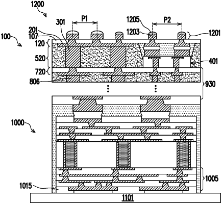
1. A method comprising:
forming a first through via over a first metallization layer;
attaching an interconnect device to the first metallization layer adjacent to the first through via;
forming a second through via over an interconnect via of the interconnect device, wherein the second through via has a first height and a first width, the second through via having a first bottom surface and a first top surface; and
forming a third through via over the first through via, wherein the third through via has the first height and a second width, the second width being different from the first width, the third through via having a second bottom surface and a second top surface, the first bottom surface being planar with the second bottom surface and the first top surface being planar with the second top surface.