| CPC H01L 21/31144 (2013.01) [H01L 21/31116 (2013.01); H01L 21/32135 (2013.01)] | 17 Claims |

|
1. A method for processing a substrate, comprising:
providing a substrate comprising a sacrificial layer and an insulative layer stacked on the sacrificial layer;
forming a polysilicon hardmask on the insulative layer;
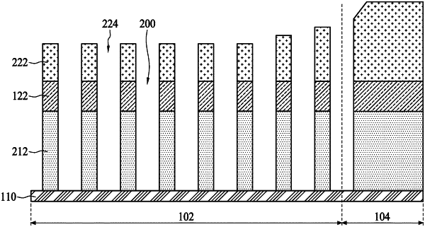
etching the insulative layer and the sacrificial layer exposed through a plurality of openings of the polysilicon hardmask to form a plurality of channels, wherein each of the channels is indented from a top surface of the polysilicon hardmask through the polysilicon hardmask, the insulative layer and the sacrificial layer;
depositing a metal film on the polysilicon hardmask and in the channels, wherein the metal film covers the top surface of the polysilicon hardmask and sidewalls of the channels;
depositing a passivation film on the metal film to cover the top surface of the polysilicon hardmask and sidewalls of the channels;
performing a first removal process to remove portions of the passivation film and the metal film above the polysilicon hardmask, wherein the passivation film and the metal film above the top surface of the polysilicon hardmask are removed after the first removal process to expose the top surface of the polysilicon hardmask;
performing a second removal process to remove portions of the polysilicon hardmask exposed through the passivation film and the metal film, wherein the polysilicon hardmask is recessed from the top surface thereof after the second removal process; and
performing a third removal process to remove the polysilicon hardmask and portions of the passivation film and the metal film surrounding the polysilicon hardmask.
|