| CPC H01L 21/31144 (2013.01) [H01L 21/31053 (2013.01); H01L 21/31116 (2013.01)] | 20 Claims |

|
1. A method for forming a three-dimensional (3D) memory device, comprising:
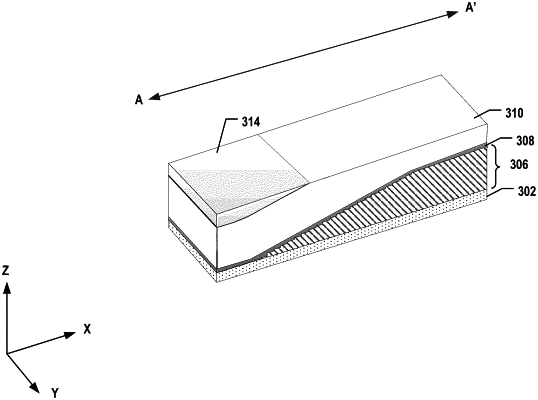
forming a stack structure over a staircase region and an array region;
forming a dielectric material layer over the array region and the staircase region;
forming an etch mask layer over the dielectric material layer;
planarizing a first surface of the etch mask layer away from the dielectric material layer to fully remove a portion of the etch mask layer over the array region and form a remaining portion of the etch mask layer over the staircase region; and
etching the dielectric material layer and the remaining portion of the etch mask layer to form a dielectric layer over the staircase region and the array region.
|
|
13. A method for forming a three-dimensional (3D) memory device, comprising:
forming a stack structure over a staircase region and an array region;
forming a dielectric material layer over the array region and the staircase region;
forming an etch mask layer over the dielectric material layer that is arranged over the array region and the staircase region, the etch mask layer comprising a first portion over the array region and a second portion over the staircase region, and the second portion of the etch mask layer being thicker than the first portion of the etch mask layer;
removing the first portion of the etch mask layer, over the array region, from the etch mask layer to form an etch mask portion over a portion of the dielectric material layer over the staircase region, the etch mask portion being part of the second portion of the etch mask layer over the staircase region; and
etching the dielectric material layer and the etch mask portion to form a dielectric layer over the staircase region and the array region.
|