| CPC H01L 21/3086 (2013.01) [H01L 21/0337 (2013.01); H01L 21/823431 (2013.01); H01L 27/0924 (2013.01); H01L 29/0665 (2013.01); H01L 29/401 (2013.01); H01L 29/66545 (2013.01)] | 20 Claims |

|
1. A semiconductor structure comprising:
a substrate;
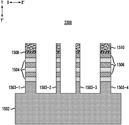
a nanosheet stack disposed over the substrate, the nanosheet stack comprising alternating layers of a sacrificial material and a channel material, the layers of channel material providing nanosheet channels for one or more nanosheet field-effect transistors;
a hard mask stack disposed over the nanosheet stack;
a patterning layer disposed over the hard mask stack; and
a lithographic mask disposed over the patterning layer, the lithographic mask defining (i) one or more first regions having a first width for direct printing of one or more fins of the first width in the nanosheet stack and the substrate and (ii) one or more second regions having a second width for setting the spacing between two or more fins of the second width in the nanosheet stack and the substrate using self-aligned double patterning;
wherein the second width is less than the first width.
|