| CPC H01L 21/28132 (2013.01) [H01L 21/28088 (2013.01); H01L 21/31111 (2013.01); H01L 29/4966 (2013.01); H01L 29/66545 (2013.01); H01L 29/6656 (2013.01); H01L 29/66795 (2013.01); H01L 29/7851 (2013.01)] | 16 Claims |
|
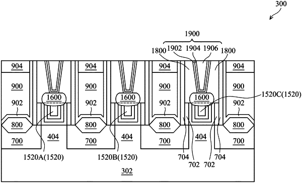
1. A semiconductor device, comprising:
a semiconductor fin;
a metal gate disposed over the semiconductor fin;
a gate dielectric layer disposed between the semiconductor fin and the metal gate;
spacers sandwiching the metal gate, wherein the spacers include a first spacer contacting the gate dielectric layer and a second spacer contacting the first spacer, the first spacer and the second spacer having different heights; and
a gate electrode contacting the metal gate and the gate dielectric layer at a first interface and a second interface, respectively, wherein the first interface is below the second interface, and wherein a top surface of the gate electrode is above a top surface of the gate dielectric layer, wherein a top surface of the first spacer is below the top surface of the gate electrode, and wherein a top surface of the second spacer is above the top surface of the gate electrode.
|