US 12,080,551 B2
SiC composite substrate including biaxially oreinted SiC layer and semiconductor device
Risa Miyakaze, Nagoya (JP); Kiyoshi Matsushima, Nagoya (JP); Jun Yoshikawa, Nagoya (JP); and Morimichi Watanabe, Nagoya (JP)
Assigned to NGK INSULATORS, LTD., Nagoya (JP)
Filed by NGK INSULATORS, LTD., Nagoya (JP)
Filed on Jun. 11, 2021, as Appl. No. 17/303,967.
Application 17/303,967 is a continuation of application No. PCT/JP2020/005741, filed on Feb. 14, 2020.
Claims priority of application No. 2019-043465 (JP), filed on Mar. 11, 2019.
Prior Publication US 2021/0301422 A1, Sep. 30, 2021
Int. Cl. C30B 23/02 (2006.01); C30B 29/36 (2006.01); H01L 21/02 (2006.01); C01B 32/956 (2017.01); H01L 29/16 (2006.01); H01L 29/161 (2006.01); H01L 29/66 (2006.01)
CPC H01L 21/0262 (2013.01) [C30B 23/02 (2013.01); C30B 29/36 (2013.01); H01L 21/02378 (2013.01); H01L 21/02433 (2013.01); H01L 21/02529 (2013.01); H01L 21/0259 (2013.01); H01L 21/02609 (2013.01); C01B 32/956 (2017.08); H01L 29/1608 (2013.01); H01L 29/161 (2013.01); H01L 29/66053 (2013.01)] 4 Claims
OG exemplary drawing
 
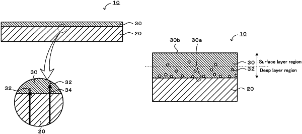
1. A SiC composite substrate comprising:
a SiC single crystal layer; and
at least one biaxially oriented SiC layer disposed on the SiC single crystal layer, wherein the at least one biaxially d SiC layer is oriented in both a c-axis direction and an a-axis direction, and wherein the at least one biaxially oriented SiC layer has pores and has a density of defect reaching the surface of the at least one biaxially oriented SiC layer of 1.0×101/cm2 or less.