| CPC G11C 7/1096 (2013.01) [G11C 7/12 (2013.01); G11C 8/08 (2013.01); H01L 29/7869 (2013.01); H10B 12/31 (2023.02); H10B 12/50 (2023.02)] | 21 Claims |

|
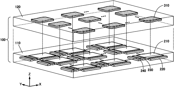
1. A semiconductor device comprising a plurality of arithmetic blocks,
wherein one of the plurality of arithmetic blocks comprises an arithmetic circuit portion in a first layer and a memory circuit portion in a second layer,
wherein the arithmetic circuit portion comprises a first driver circuit, a second driver circuit and a third driver circuit in the first layer,
wherein each of the first driver circuit, the second driver circuit and the third driver circuit is electrically connected to the memory circuit portion, and
wherein the memory circuit portion and each of the first driver circuit, the second driver circuit and the third driver circuit overlap each other.
|