| CPC G11C 5/148 (2013.01) | 20 Claims |

|
1. A device comprising:
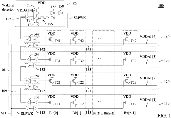
a first virtual power line, in a first memory bank, configured to be coupled to a power supply through a first group of transistor switches;
a second virtual power line, in a second memory bank, configured to receive the power supply through a second group of transistor switches;
a first delay circuit having a first input coupled to gate terminals of the first group of transistor switches and having a first output coupled to gate terminals in the second group of transistor switches;
a first wakeup detector configured to generate a first trigger signal after receiving a signal from the first output of the first delay circuit; and
a plurality of main input-output (MIO) controllers configured to be coupled to the power supply through a first group of wakeup switches and through a first group of function switches, wherein gate terminals in the first group of wakeup switches are configured to receive the first trigger signal.
|