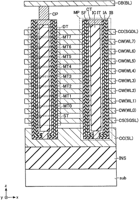
| CPC G11C 16/3459 (2013.01) [G11C 7/08 (2013.01); G11C 7/1063 (2013.01); G11C 16/102 (2013.01); G11C 16/26 (2013.01)] | 18 Claims |

|
1. A memory device comprising:
a first conductor;
a first semiconductor extending along a first axis and in contact with the first conductor at an end;
a first layer that is spaced from the first semiconductor, extends along the first axis, and is made of an insulator;
a second conductor facing the first conductor and sandwiching the first layer together with the first semiconductor;
a third conductor sandwiching the first layer together with the first semiconductor and positioned farther from the first conductor than the second conductor is;
a fourth conductor that sandwiches the first layer together with the first semiconductor, is positioned farther from the first conductor than the third conductor is, and is aligned with the third conductor;
a first circuit configured to apply a first potential to the first conductor, apply a second potential lower than the first potential to the third conductor in parallel with the application of the first potential, and apply a third potential higher than the second potential and lower than the first potential to the fourth conductor in parallel with the application of the first potential;
a sixth conductor sandwiching the first layer together with the first semiconductor and positioned between the second conductor and the third conductor;
a seventh conductor sandwiching the first layer together with the first semiconductor and positioned between the sixth conductor and the third conductor;
an eighth conductor sandwiching the first layer together with the first semiconductor and positioned farther from the first conductor than the fourth conductor is; and
a ninth conductor positioned farther from the first conductor than the seventh conductor is, and aligned with the seventh conductor,
wherein:
the first circuit is further configured to:
apply a seventh potential to the second conductor and the eighth conductor,
apply an eighth potential to the seventh conductor in parallel with the application of the seventh potential,
apply a ninth potential higher than the eighth potential to the sixth conductor in parallel with the application of the seventh potential,
apply a tenth potential lower than the ninth potential to the third conductor in parallel with the application of the seventh potential,
apply an eleventh potential higher than the tenth potential and lower than the ninth potential to the fourth conductor in parallel with the application of the seventh potential, and
apply the ninth potential to the ninth conductor in parallel with the application of the seventh potential.
|