| CPC G11C 16/3427 (2013.01) [G11C 16/0483 (2013.01); G11C 16/10 (2013.01); G11C 16/24 (2013.01)] | 20 Claims |
|
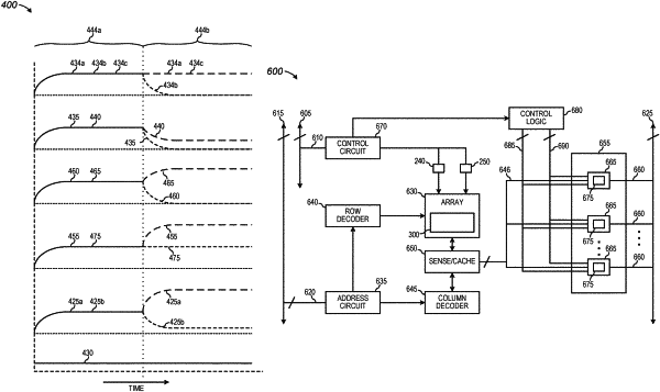
1. A method, comprising:
programming a memory cell in a block of NAND memory cell strings, the block including multiple sub-blocks of memory cell strings, wherein the memory cell strings respectively comprise multiple NAND memory cells extending between a source select gate and a drain select gate and sharing a common channel material;
wherein the programming of a selected NAND memory cell in a selected NAND memory cell string in a selected sub-block, comprises:
during a first interval of a programming operation, precharging channel material of memory cell strings in both the selected sub-block and in at least one unselected sub-block to a precharge voltage, wherein the at least one unselected sub-block does not contain a selected memory cell; and
during a second interval of the programming operation, after the first interval, applying a programming voltage to a first access line coupled to the selected memory cell in the selected sub-block, wherein an unselected memory cell in the at least one unselected sub-block is also coupled to the first access line;
wherein during the second interval of the programming operation, the channel materials of a group of memory cell strings in the unselected sub-block are charged to a first voltage higher than the precharge voltage by a voltage induced on the channel materials of the group of memory cell strings in the unselected sub-block as a result of the programming voltage on the first access line.
|