| CPC G11C 16/26 (2013.01) [G11C 16/0483 (2013.01)] | 25 Claims |
|
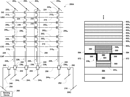
1. A method of forming an integrated circuit structure for a capacitive sense NAND memory, the method comprising:
forming a first semiconductor overlying a dielectric;
forming a second semiconductor to be in contact with a first end of the first semiconductor, and forming a third semiconductor to be in contact with a second end of the first semiconductor opposite the first end of the first semiconductor;
forming a vertical channel material structure overlying the first semiconductor and having a channel material capacitively coupled to the first semiconductor; and
forming a plurality of series-connected field-effect transistors adjacent the vertical channel material structure.
|