| CPC G11C 16/16 (2013.01) [G11C 16/14 (2013.01); G11C 16/26 (2013.01); G11C 16/344 (2013.01); G11C 16/3445 (2013.01)] | 10 Claims |

|
1. A nonvolatile semiconductor memory device comprising:
a bit line;
a plurality of first word lines;
a plurality of second word lines;
a source line;
a memory block including a plurality of memory cells connected in series, the memory cells including:
a first part of the memory cells, to gates of which the first word lines are connected, respectively; and
a second part of the memory cells, to gates of which the second word lines are connected, respectively, the second part of the memory cells functioning as dummy memory cells; and
a control unit configured to:
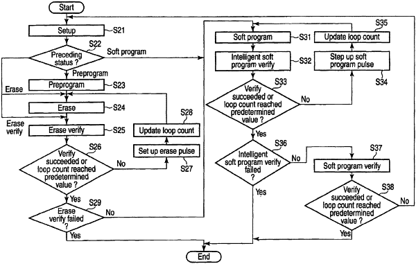
perform an erase operation upon receipt of an erase command, the erase operation including:
a plurality of erase voltage apply steps applied to the first part of the memory cells and the second part of the memory cells;
a plurality of erase verify steps applied to the first part of the memory cells and the second part of the memory cells, the erase verify steps each performed after a corresponding one of the erase voltage apply steps;
a soft program step applied only to the second part of the memory cells; and
a soft program verify step applied only to the second part of the memory cells, the soft program verify step performed after the soft program step;
suspend the erase operation upon receipt of a suspend command during performing one of the erase voltage apply steps, the erase operation being suspended at completion of one of the erase voltage apply steps;
perform a first operation upon receipt of a first command, an operation time of the erase operation being longer than an operation time of the first operation; and
resume the erase operation upon receipt of a resume command, the erase operation being resumed at start of one of the erase verify steps.
|