| CPC G11C 16/16 (2013.01) [G11C 16/0483 (2013.01); G11C 16/3445 (2013.01)] | 13 Claims |
|
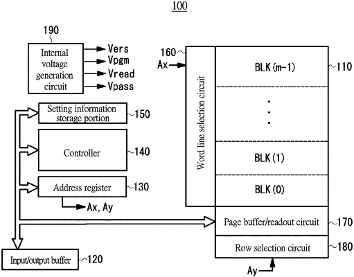
8. A semiconductor device, comprising a NAND memory cell array; and
an erasing component erasing a selected block of the memory cell array,
wherein the erasing component performs a first erasing verification on the selected block with a first readout voltage, performs a second erasing verification with a second readout voltage lower than the first readout voltage, controls a next erase pulse to be applied based on the first erasing verification and the second erasing verification, and applies an erase pulse with a same erase voltage as last time between thresholds specified by the first erasing verification and the second erasing verification.
|