| CPC G11C 11/40618 (2013.01) [G11C 11/40611 (2013.01); G11C 11/4096 (2013.01)] | 20 Claims |

|
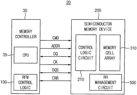
1. A semiconductor memory device, comprising:
a memory cell array comprising a plurality of memory cell rows, each comprising a plurality of memory cells;
a row hammer management circuit configured to count a number of times of access associated with each of the plurality of memory cell rows in response to receiving an active command from an external memory controller,
wherein counted values corresponding to the counted number of times are stored in count cells of each of the plurality of memory cell rows as count data,
wherein the row hammer management circuit comprises a hammer address queue configured to:
store one or more candidate hammer addresses up to a first number based on a first-in first-out (FIFO) scheme, which are intensively accessed, from among the plurality of memory cell rows, based on a comparison of the counted values with a first reference number of times;
in response to a number of the candidate hammer addresses stored in the hammer address queue reaching a second number equal to or smaller than the first number, transition a logic level of an error signal provided to the memory controller; and
in response to the number of the candidate hammer addresses stored in the hammer address queue reaching the first number, output one of the candidate hammer addresses stored in the hammer address queue as a hammer address; and
a refresh control circuit configured to receive the hammer address and to perform a hammer refresh operation on one or more victim memory cell rows which are physically adjacent to a memory cell row from among the plurality of memory cell rows corresponding to the hammer address.
|