| CPC G09G 3/3266 (2013.01) [G09G 3/20 (2013.01); G11C 19/20 (2013.01); G11C 19/28 (2013.01); G09G 3/3233 (2013.01); G09G 2300/0426 (2013.01); G09G 2300/0819 (2013.01); G09G 2300/0842 (2013.01); G09G 2300/0861 (2013.01); G09G 2310/0286 (2013.01); G09G 2310/061 (2013.01); G09G 2310/08 (2013.01)] | 20 Claims |
|
1. A display panel, comprising:
a driving circuit, including N levels of shift registers cascaded with each other, N≥2; and
a shift register of the N levels of the shift registers including:
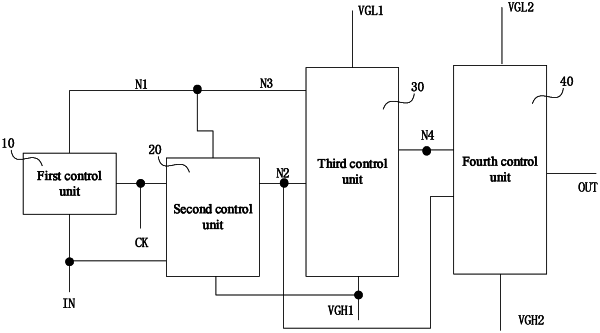
a third control unit, configured to receive the first voltage signal and a second voltage signal and control a signal of a fourth node in response to the signal of the second node and a signal of a third node, wherein the first voltage signal is a high-level signal and the second voltage signal is a low-level signal; and
a fourth control unit, configured to receive a third voltage signal and a fourth voltage signal and generate an output signal in response to the signal of the first node and the signal of the fourth node and including a first transistor and a second transistor, the third voltage signal being a high level signal, and the fourth voltage signal being a low level signal, wherein:
the first transistor and the second transistor are PMOS P-type transistors, a source of the first transistor is connected to the third voltage signal, a drain of the first transistor is connected to the output signal, a gate of the first transistor is connected to the fourth node, a source of the second transistor is connected to the fourth voltage signal, a drain of the second transistor is connected to the output signal, and a gate of the second transistor is connected to the second node, or the source of the first transistor is connected to the third voltage signal, the drain of the first transistor is connected to the output signal, the gate of the first transistor is connected to the second node, the source of the second transistor is connected to the fourth voltage signal, the drain of the second transistor is connected to the output signal, and the gate of the second transistor is connected to the fourth node; or
the first transistor and the second transistor are N-type transistors, the source of the first transistor is connected to the fourth voltage signal, the drain of the first transistor is connected to the output signal, the gate of the first transistor is connected to the fourth node, the source of the second transistor is connected to the third voltage signal, the drain of the second transistor is connected to the output signal, and the gate of the second transistor is connected to the second node, or the source of the first transistor is connected to the fourth voltage signal, the drain of the first transistor is connected to the output signal, the gate of the first transistor is connected to the second node, the source of the second transistor is connected to the third voltage signal, the drain of the second transistor is connected to the output signal, and the gate of the second transistor is connected to the fourth node.
|