| CPC G09G 3/3266 (2013.01) [G09G 3/3233 (2013.01); G09G 3/3275 (2013.01); G09G 2310/08 (2013.01); G09G 2320/0257 (2013.01)] | 13 Claims |

|
1. A display device comprising:
in a display region,
a first scanning control line,
a light emission control line extending parallel to the first scanning control line,
a data signal line intersecting the first scanning control line,
a pixel circuit provided at an intersection of the first scanning control line and the data signal line, and
a light-emitting element provided for each of the pixel circuits; and
in a non-display region,
a first scanning control circuit configured to drive the first scanning control line and
a light emission control circuit configured to drive the light emission control line,
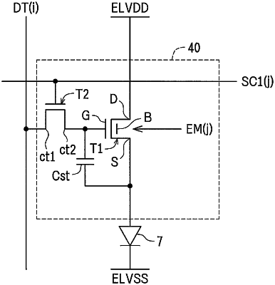
wherein each of the pixel circuits includes a drive transistor, a write transistor, and a capacitor configured to hold a data signal, the drive transistor including a first control terminal and a second control terminal positioned above and below a semiconductor layer with the semiconductor layer interposed between the first and second control terminals, the drive transistor configured to cause a drive current to flow to the light-emitting element,
the write transistor includes a first conduction terminal connected to the data signal line, a second conduction terminal connected to the first control terminal of the drive transistor, and a control terminal connected to the first scanning control line,
the drive transistor includes the second control terminal connected to the light emission control line,
the light emission control circuit outputs, to the light emission control line, a light emission control signal that switches between a select state in which the drive transistor is turned on and a non-select state in which the drive transistor is turned off,
the display region includes an initialization power supply line and a second scanning control line extending parallel to the first scanning control line, and the non-display region includes a second scanning control circuit configured to drive the second scanning control line,
the pixel circuit includes an initialization transistor, the initialization transistor including a first conduction terminal connected to the initialization power supply line, a second conduction terminal connected to a conduction terminal of the drive transistor on the light-emitting element side, and a control terminal connected to the second scanning control line,
a first counter electrode of the capacitor is connected to the first control terminal of the drive transistor, and a second counter electrode of the capacitor is connected to the second conduction terminal of the initialization transistor,
in a period before a write period of the data signal with respect to the capacitor, the second scanning control circuit sets the second scanning control line to be in a select state to turn on the initialization transistor, and an initialization voltage of the initialization power supply line is applied to the second counter electrode of the capacitor,
in the write period of the data signal with respect to the capacitor, the first scanning control circuit sets the first scanning control line to be in a select state to turn on the write transistor, the second scanning control circuit sets the second scanning control line to be in a non-select state to turn off the initialization transistor, and the light emission control circuit sets the light emission control line to be in the non-select state to turn off the drive transistor, and the data signal is applied to the first counter electrode of the capacitor, and
in a period from the write period to a light emission period, the first scanning control circuit maintains the first scanning control line in a non-select state to keep the write transistor off, the second scanning control circuit maintains the non-select state of the second scanning control line to keep the initialization transistor off, and the light emission control circuit sets the light emission control line to be in the select state to turn on the drive transistor.
|