| CPC G09G 3/3233 (2013.01) [G09G 2300/0426 (2013.01); G09G 2300/0819 (2013.01); G09G 2310/0202 (2013.01); G09G 2310/08 (2013.01); G09G 2320/0238 (2013.01); G09G 2320/045 (2013.01)] | 6 Claims |

|
1. An electro-optical device comprising:
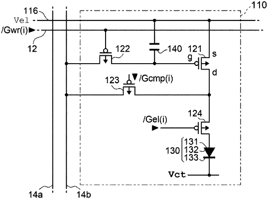
a pixel circuit provided corresponding to a scanning line and a data line, wherein
the pixel circuit includes:
a first transistor being configured to supply the light emitting element with a current corresponding to a voltage between a gate node of the first transistor and a source node of the first transistor;
a second transistor electrically connecting the data line and the gate node of the first transistor, and is in an ON state or an OFF state in accordance with a voltage of the scanning line;
a third transistor electrically connecting the data line and the drain node of the first transistor,
a fourth transistor electrically connecting the drain node of the first transistor and the light emitting element; and
a light emitting element,
a horizontal scanning period sequentially includes a compensation period, a first period, and a second period,
in the compensation period, the second transistor and the third transistor are in the ON state, the gate node of the first transistor and a drain node of the first transistor are electrically coupled, and a voltage of the gate node of the first transistor is a voltage corresponding to a threshold voltage of the first transistor,
in the first period, the second transistor is in the ON state, and the third transistor is in the OFF state, a voltage corresponding to luminance of the light emitting element is applied to the gate node of the first transistor and the voltage of the gate node of the first transistor is varied from the voltage corresponding to the threshold voltage to the voltage corresponding to luminance of the light emitting element,
in the second period, the second transistor is in the OFF state, and the third transistor is in the ON state, the voltage corresponding to the luminance of the light emitting element is applied to the drain node of the first transistor.
|