| CPC G09G 3/3233 (2013.01) [G09G 3/3266 (2013.01); G09G 3/32 (2013.01); G09G 2300/0408 (2013.01); G09G 2300/0426 (2013.01); G09G 2300/0842 (2013.01); G09G 2310/0202 (2013.01); G09G 2310/0267 (2013.01); G09G 2310/08 (2013.01); G09G 2320/0257 (2013.01); G09G 2320/0261 (2013.01)] | 24 Claims |

|
1. A display device, comprising:
a substrate;
a plurality of driving transistors on the substrate;
a plurality of anode electrodes connected with the plurality of driving transistors;
a light emitting layer on the plurality of anode electrodes; and
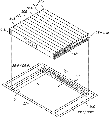
a plurality of split cathode electrodes on the light emitting layer,
wherein each of the plurality of split cathode electrodes alternates between a first state applied with a cathode voltage and a second state of floating not applied with the cathode voltage,
wherein the display device further comprises:
at least one cathode voltage line receiving the cathode voltage;
a plurality of control switching elements respectively corresponding to the plurality of split cathode electrodes, the plurality of control switching elements configured to switch a connection between each of the plurality of split cathode electrodes and the at least one cathode voltage line; and
a plurality of cathode driving circuits respectively corresponding to the plurality of control switching elements, the plurality of cathode driving circuits configured to output a plurality of control gate signals for controlling a turn on and a turn off of each of the plurality of control switching elements to the plurality of control switching elements, respectively,
wherein the plurality of cathode driving circuits include an nth cathode driving circuit,
wherein the nth cathode driving circuit includes a cathode pull-up transistor and a cathode pull-down transistor configured to output an nth control gate signal,
wherein a gate node of the cathode pull-up transistor is electrically connected with a first Q node, and a gate node of the cathode pull-down transistor is electrically connected with a first QB node.
|