| CPC G09G 3/32 (2013.01) [G09G 2300/0426 (2013.01); G09G 2320/0257 (2013.01); G09G 2320/043 (2013.01)] | 21 Claims |

|
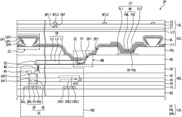
1. A display panel, comprising:
a transistor;
a light-emitting element including:
a first electrode;
a light emitting layer disposed on the first electrode; and
a second electrode disposed on the light emitting layer, the second electrode being electrically connected to the transistor;
an insulating layer disposed between the transistor and the light-emitting element; and
a connection wiring electrically connecting the transistor and the second electrode to each other, wherein
the connection wiring includes:
a first contact electrically connected to the second electrode; and
a second contact electrically connected to the transistor,
the first contact includes:
a first layer;
a second layer disposed on the first layer; and
a third layer disposed on the second layer,
the second layer including a second side end disposed between the first layer and the third layer, and
the second side end includes:
a first portion spaced apart from a third side end of the third layer by a first spacing in a plan view of the display panel; and
a second portion spaced apart from the third side end by a second spacing larger than the first spacing in the plan view.
|