| CPC G09G 3/32 (2013.01) [G09G 3/3208 (2013.01); G09G 3/3233 (2013.01); G09G 3/3266 (2013.01); G09G 2300/0426 (2013.01); G09G 2300/0809 (2013.01); G09G 2300/0819 (2013.01); G09G 2300/0842 (2013.01); G09G 2300/0861 (2013.01); G09G 2310/0286 (2013.01); G09G 2310/061 (2013.01); G09G 2310/08 (2013.01); G09G 2320/0233 (2013.01); G09G 2330/021 (2013.01); G11C 19/28 (2013.01)] | 17 Claims |
|
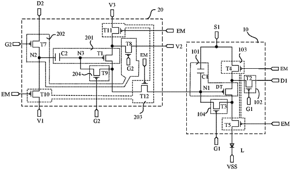
1. A pixel driving circuit, comprising:
a driving control sub-circuit connected at least to a first scanning signal terminal, a first data signal terminal, a first power supply voltage signal terminal, an enable signal terminal, and a first electrode of an element to be driven, wherein the driving control sub-circuit includes a first driving sub-circuit, and the driving control sub-circuit is configured to: write at least a first data signal from the first data signal terminal into the first driving sub-circuit in response to a first scanning signal received from the first scanning signal terminal; and make the first driving sub-circuit output a driving signal according to the first data signal and a first power supply voltage signal from the first power supply voltage signal terminal in response to an enable signal received from the enable signal terminal, so as to drive the element to be driven to operate; and
a time control sub-circuit including:
a second driving sub-circuit including a first transistor and a second capacitor, wherein a first electrode of the second capacitor is connected to a second node, and a second electrode of the second capacitor is connected to a third node; and a gate of the first transistor is connected to the third node;
a second data writing sub-circuit connected to a second scanning signal terminal, a second voltage signal terminal, a second data signal terminal, the second node, and a first electrode of the first transistor, wherein the second data writing sub-circuit is configured to write a second data signal from the second data signal terminal into the second node, and write a second voltage signal from the second voltage signal terminal into the first electrode of the first transistor, in response to a second scanning signal received from the second scanning signal terminal;
a second threshold voltage compensation sub-circuit connected to the second scanning signal terminal, a second electrode of the first transistor, and the third node, wherein the second threshold voltage compensation sub-circuit is configured to transmit the second voltage signal and a threshold voltage of the first transistor to the third node, in response to the second scanning signal received from the second scanning signal terminal; and
a second control sub-circuit connected to the enable signal terminal, a first voltage signal terminal, a third voltage signal terminal, the first driving sub-circuit, the second node, and the first transistor, wherein the second control sub-circuit is configured to transmit a first voltage signal varying within a set voltage range from the first voltage signal terminal to the second node, and make the first transistor be electrically connected with the third voltage signal terminal and the first driving sub-circuit, in response to the enable signal received from the enable signal terminal; wherein
the second driving sub-circuit is configured to output a third voltage signal from the third voltage signal terminal to the first driving sub-circuit at least in response to the second data signal and a change in voltage of the first voltage signal, so as to make the first driving sub-circuit stop outputting the driving signal, and control operating duration of the element to be driven.
|