| CPC G09G 3/32 (2013.01) [H01L 27/156 (2013.01); H01L 33/60 (2013.01); G09G 2300/0408 (2013.01); G09G 2300/0426 (2013.01); G09G 2300/0819 (2013.01); G09G 2300/0852 (2013.01); G09G 2300/0861 (2013.01); G09G 2310/0202 (2013.01); G09G 2310/08 (2013.01); G09G 2320/0233 (2013.01); G09G 2320/0252 (2013.01); G09G 2320/045 (2013.01)] | 26 Claims |

|
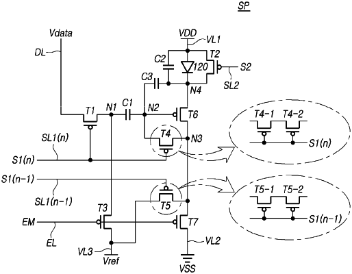
1. A display device, comprising:
a light emitting element; and
a pixel circuit connected to the light emitting element, the pixel circuit including a driving transistor having a gate electrode, a source electrode, and a drain electrode, a first transistor including a source electrode connected to a data line and a drain electrode, and a capacitor connected with the gate electrode of the driving transistor and the drain electrode of the first transistor,
wherein a driving period of the pixel circuit includes:
a first period during which a reference voltage is applied to the gate electrode of the driving transistor;
a second period during which a gate-source voltage difference of the driving transistor is a threshold voltage of the driving transistor;
a third period during which the reference voltage is applied to the capacitor and a voltage of the gate electrode of the driving transistor varies due to a coupling phenomenon of the capacitor;
a fourth period during which a high-potential voltage is applied to the source electrode, the high-potential voltage greater than the reference voltage; and
a fifth period during which the driving transistor is turned on and the light emitting element emits light.
|