| CPC G09G 3/32 (2013.01) [G09G 3/3266 (2013.01); G09G 3/3208 (2013.01); G09G 2300/0408 (2013.01); G09G 2300/0426 (2013.01); G09G 2300/0809 (2013.01); G09G 2310/0267 (2013.01); G09G 2310/0286 (2013.01); G09G 2320/0223 (2013.01)] | 20 Claims |
|
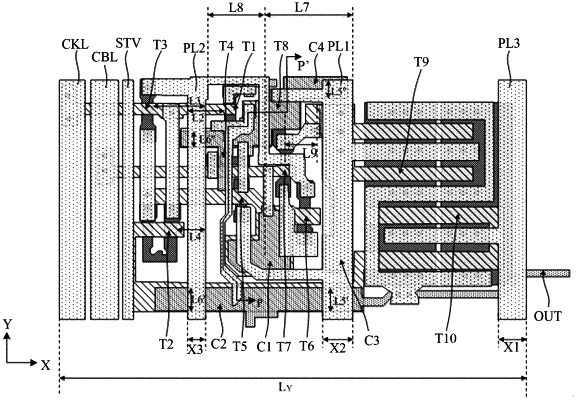
1. A display substrate, comprising:
a base substrate;
a scan drive control circuit disposed in a non-display area of the base substrate;
the scan drive control circuit comprises an input circuit, an output control circuit and an output circuit; the output control circuit is connected to the input circuit and the output circuit;
the output control circuit comprises a first node control capacitor and a second node control capacitor;
lengths of the first node control capacitor, the second node control capacitor and the scan drive control circuit in a first direction satisfy:
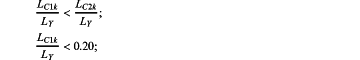 where, LC1k is a length of the first node control capacitor in the first direction, LC2k is a length of the second node control capacitor in the first direction, LY is a length of the scan drive control circuit in the first direction.
|