| CPC G09G 3/32 (2013.01) [G09G 3/006 (2013.01); G09G 2300/0426 (2013.01); G09G 2300/0819 (2013.01); G09G 2300/0852 (2013.01); G09G 2300/0861 (2013.01); G09G 2310/0267 (2013.01); G09G 2330/12 (2013.01)] | 21 Claims |
|
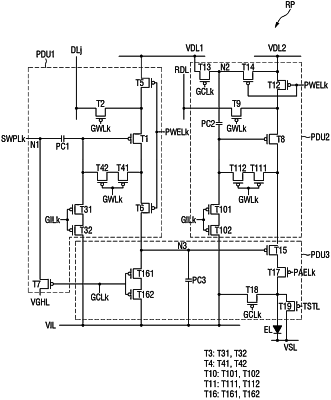
1. A display device comprising:
a sub-pixel connected to a scan write line, a first data line, and a second data line, wherein the sub-pixel comprises:
a light emitting element;
a first pixel driving unit configured to generate a control current according to a first data voltage of the first data line;
a second pixel driving unit configured to generate a driving current applied to the light emitting element according to a second data voltage of the second data line; and
a third pixel driving unit configured to apply the driving current to the light emitting element according to the control current of the first pixel driving unit,
wherein the first pixel driving unit comprises:
a first transistor configured to generate the control current according to the first data voltage;
a second transistor configured to apply the first data voltage of the first data line to a first electrode of the first transistor according to a scan write signal of the scan write line; and
a third transistor connecting a gate electrode and a second electrode of the first transistor according to the scan write signal of the scan write line,
wherein the third transistor comprises a first sub-transistor and a second sub-transistor connected in series between the gate electrode and the second electrode of the first transistor, and
wherein a channel of the first sub-transistor and a channel of the second sub-transistor overlap a bottom gate electrode of the third transistor.
|