| CPC G09G 3/32 (2013.01) [G09G 2300/0842 (2013.01); G09G 2310/0275 (2013.01)] | 20 Claims |

|
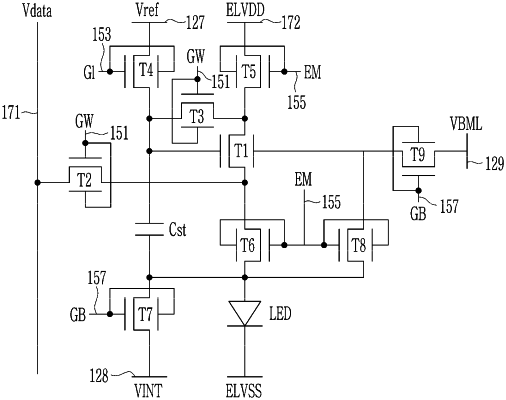
1. An emissive display device comprising:
a light emitting diode comprising an anode;
an n-type driving transistor comprising a first driving gate electrode, a first electrode configured to receive a driving voltage, a second electrode configured to transfer an output current to the anode, and a second driving gate electrode;
a second transistor comprising a first electrode connected to a data line;
a third transistor configured to connect the first electrode of the driving transistor and the first driving gate electrode of the driving transistor;
a storage capacitor comprising a first storage electrode and a second storage electrode connected to the first driving gate electrode;
a ninth transistor configured to transfer an overlapping electrode voltage to the second driving gate electrode;
an overlapping electrode voltage line configured to cross the data line in a plan view and to receive the overlapping electrode voltage; and
a shielding electrode at an intersection of the data line and the overlapping electrode voltage line and positioned between the data line and the overlapping electrode voltage line in a cross-sectional view.
|