| CPC G09G 3/2096 (2013.01) [G09G 3/3233 (2013.01); G09G 2300/0819 (2013.01); G09G 2300/0842 (2013.01); G09G 2310/08 (2013.01); G09G 2320/0233 (2013.01); G09G 2320/043 (2013.01); G09G 2330/021 (2013.01); G09G 2330/028 (2013.01); G09G 2360/16 (2013.01); H01L 25/167 (2013.01)] | 19 Claims |

|
1. A display device comprising:
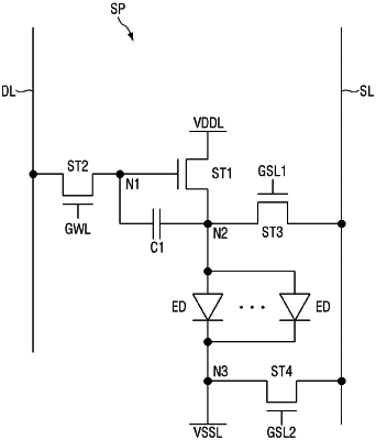
pixels arranged along rows and columns, and comprising:
light-emitting elements;
a first transistor for supplying a driving current to the light-emitting elements;
a second transistor for supplying a data voltage to a first node at a gate electrode of the first transistor upon receiving a scan write signal of a gate high level during a first period;
a third transistor for electrically connecting a second node, which is at a first electrode, and a sensing line upon receiving a first scan sensing signal of a gate high level during the first period and during a second period after the first period; and
a fourth transistor for electrically connecting a third node, which is at a second electrode, and the sensing line upon receiving a second scan sensing signal of a gate high level during a third period; and
a display driver for driving the pixels, for sensing voltages of the second node and the third node to calculate a driving voltage across the light-emitting elements, and for compensating for the data voltage in case that the driving voltage exceeds a reference voltage,
wherein the first period, the second period, and the third period are in a same frame.
|