| CPC G09G 3/2092 (2013.01) [G09G 2310/0267 (2013.01); G09G 2310/08 (2013.01); G09G 2320/0233 (2013.01)] | 18 Claims |
|
1. A display device, comprising:
a processor configured to output driving signals and voltages;
a timing controller connected to the processor, and configured to generate control signals based on the driving signals;
a circuit board connected to the timing controller, and configured to generate initial clock signals according to the voltages and the control signals, wherein any one of the initial clock signals is a signal with high levels and low levels that occur alternatively;
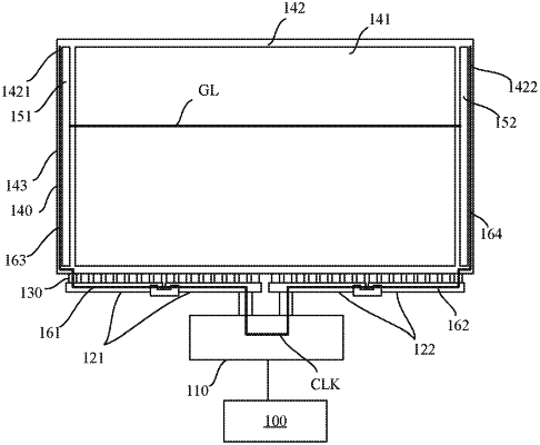
a display panel connected to the circuit board, and comprising a display area and a non-display area;
a plurality of clock signal lines configured to transmit the initial clock signals, wherein each of the clock signal lines extends from the circuit board to the non-display area of the display panel;
a plurality of grounding resistors disposed on the circuit board, wherein each of the grounding resistors is connected to a corresponding clock signal line, and is configured to reduce a voltage value of the high level of the initial clock signal to obtain an adjusted clock signal;
a gate driver disposed in the non-display area of the display panel, connected to the clock signal lines, and configured to generate a gate signal according to the adjusted clock signal; and
a gate line disposed in the display area of the display panel, connected to the gate driver, and configured to transmit the gate signal;
wherein the display device comprises a M-th clock signal line, a (M−1)th clock signal line, and a (M−2)th clock signal line arranged in sequence; and
a value of a grounding resistor of the plurality of grounding resistors connected to the M-th clock signal line is R(M), a value of a grounding resistor of the plurality of grounding resistors connected to the (M−1)th clock signal line is R(M−1), and a value of a grounding resistor of the plurality of grounding resistors connected to the (M−2)th clock signal line is R(M−2), wherein R(M)<R(M−1)<R(M−2) or R(M)>R(M−1)>R(M−2).
|