| CPC G09F 9/3026 (2013.01) [G02F 1/133314 (2021.01); G02F 1/133322 (2021.01); G02F 1/13336 (2013.01); G06F 1/1601 (2013.01); H05K 5/0217 (2013.01); H10K 59/18 (2023.02); G02F 2201/07 (2013.01); G02F 2201/46 (2013.01); G02F 2201/48 (2013.01); G02F 2202/28 (2013.01); G06F 2200/1635 (2013.01); H05K 5/0021 (2013.01)] | 16 Claims |
|
1. A display device, comprising:
a display panel;
a display element disposed in the display panel;
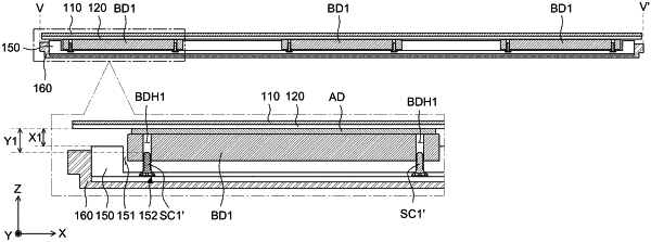
a protection plate disposed to cover a front surface of the display panel;
a frame disposed on a rear surface of the display panel and including a plurality of grooves and a plurality of holes;
a plurality of first binders bonded to the rear surface of the display panel and disposed in the plurality of grooves;
a plurality of second binders bonded to the rear surface of the display panel and disposed inside the plurality of holes;
a plurality of first coupling members penetrating the frame and coupled to the plurality of first binders;
a plurality of second coupling members penetrating the frame and coupled to the plurality of second binders; and
a plurality of adhesive members disposed between the plurality of first binders and the display panel, and between the plurality of second binders and the display panel,
wherein the display panel is an inorganic light emitting display panel, and the display element is a light emitting diode (LED) or a micro LED including an n-type semiconductor layer, a p-type semiconductor layer, and an emission layer.
|