| CPC G06V 40/1365 (2022.01) [G06F 3/0412 (2013.01); G06V 40/1318 (2022.01); H04N 25/75 (2023.01)] | 6 Claims |

|
1. An imaging device comprising:
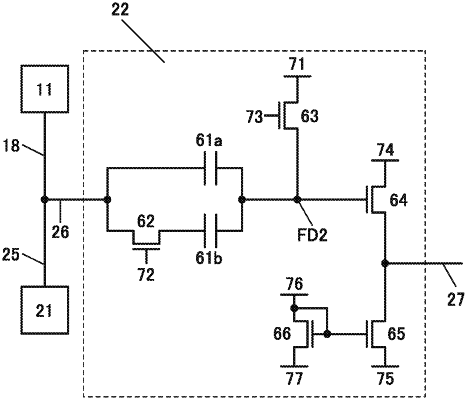
a pixel and a CDS circuit,
wherein the CDS circuit includes a first transistor, a second transistor, a third transistor, a first capacitor, and a second capacitor,
wherein the pixel is electrically connected to one of a source and a drain of the first transistor and one electrode of the first capacitor through a wiring,
wherein the other of the source and the drain of the first transistor is electrically connected to one electrode of the second capacitor, and
wherein one of a source and a drain of the second transistor is directly connected to a gate of the third transistor, the other electrode of the first capacitor, and the other electrode of the second capacitor.
|