| CPC G06F 30/39 (2020.01) [H01L 21/67144 (2013.01); H01L 21/6835 (2013.01); H01L 25/0657 (2013.01); H01L 25/50 (2013.01); G06F 2111/14 (2020.01); G06F 2113/18 (2020.01); H01L 2221/68327 (2013.01); H01L 2221/68363 (2013.01); H01L 2221/68381 (2013.01); H01L 2225/06544 (2013.01)] | 32 Claims |

|
1. A method to fabricate semiconductor devices with die sizes larger than 900 mm2, the method comprising:
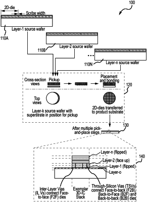
providing a first type of source wafers that contain high-resolution circuit elements partitioned into a multitude of pre-fabricated blocks (PFBs), wherein each PFB is at most 900 mm2 in size;
providing a second type of source wafers that contain lower-resolution circuit elements partitioned into a multitude of PFBs, wherein each PFB is at most 1500 mm2 in size;
assembling PFBs from the first type of source wafers onto a product substrate, followed by assembling PFBs from the second type of source wafers onto previously assembled PFBs, wherein the fully-assembled group of high-resolution and low-resolution PFBs is equivalent in function to a monolithically constructed SoC but arbitrarily larger in size than 900 mm2.
|