| CPC G06F 3/0625 (2013.01) [G06F 3/0659 (2013.01); G06F 3/0673 (2013.01)] | 16 Claims |

|
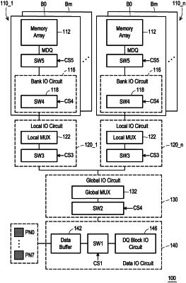
1. A memory device, comprising:
at least one memory bank, comprising a plurality of memory cells;
a plurality of data pins, coupled to a plurality of package pins, wherein the plurality of package pins correspond to a first bit order, and the plurality of data pins correspond to a second bit order;
a data input/output (IO) circuit, configured to communicate a first data with the plurality of data pins, wherein the first data is arranged in the first bit order;
at least one bank IO circuit, configured to communicate a second data with the at least one memory bank, wherein the second data is arranged in the second bit order;
a plurality of switches, configured to perform at least one swapping operation on the first data to generate the second data or to perform the at least one swapping operation on the second data to generate the first data;
a data buffer, coupled to the plurality of data pins, configured to communicate the first data with the plurality of data pins; and
a data output block IO circuit, coupled to the data buffer via the first switch,
wherein the plurality of switches are controlled by a plurality of control signals, the plurality of switches comprises a first switch, the plurality of control signals comprises a first control signal, and the first switch is configured to receive the first data from the data buffer, perform a first swapping operation on the first data according to the first control signal to generate a third data, and output the third data to the data output block IO circuit.
|