| CPC G06F 3/0611 (2013.01) [G06F 3/0653 (2013.01); G06F 3/0679 (2013.01)] | 20 Claims |
|
1. A system comprising:
a memory device comprising a memory array, the memory array comprising a plurality of memory cells; and
a processing device coupled to the memory device, the processing device to perform operations comprising:
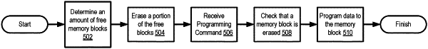
determining a value of a metric associated with a program-erase cycle (PEC) of one or more memory blocks of the memory array, wherein the memory array further comprises a plurality of memory blocks, and wherein a first memory block comprises a first set of memory cells of the plurality of memory cells;
responsive to determining that the value of the metric is below a predetermined threshold, initiating an erase protocol of the memory device;
erasing less than a predetermined portion of free sets of memory cells associated with one or more free memory blocks of the plurality of memory blocks;
subsequent to erasing less than the predetermined portion of free sets of memory cells, receiving a programming command directed to the first set of memory cells; and
performing a programming operation with respect to the first set of memory cells responsive to receiving the programming command.
|