| CPC G06F 3/044 (2013.01) [G06F 3/0412 (2013.01); G06F 3/0416 (2013.01); G06V 40/1306 (2022.01); G09G 3/20 (2013.01); G09G 3/2092 (2013.01); H10K 59/40 (2023.02); G06F 2203/04103 (2013.01); G06F 2203/04111 (2013.01); G09G 2300/0426 (2013.01)] | 20 Claims |

|
1. A display device comprising:
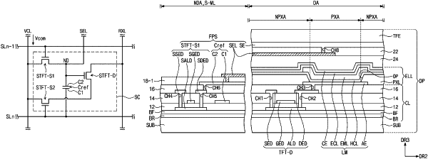
a display panel including a display area having a pixel and a non-display area disposed adjacent to the display area, the pixel including a first thin film transistor disposed within layers of the display panel;
a fingerprint sensor including a sensing electrode overlapping the display area and a sensing circuit including a second thin film transistor disposed within the same layers of the display panel;
a first pad electrically connected to the display panel; and
a second pad electrically connected to the fingerprint sensor,
wherein the first pad and the second pad are disposed in the non-display area and are spaced apart from each other with the display area interposed therebetween.
|
|
14. A display device comprising:
a display panel including a display area having a pixel and a non-display area disposed adjacent to the display area, the pixel including a first thin film transistor disposed within layers of the display panel;
a fingerprint sensor including a sensing electrode overlapping the display area and a sensing circuit including a second thin film transistor electrically connected to the sensing electrode and disposed within the same layers of the display panel;
a gate driving circuit disposed in the non-display area and electrically connected to the pixel; and
a scan driving circuit disposed in the non-display area and electrically connected to the sensing circuit,
wherein the sensing electrode and the sensing circuit are spaced apart from each other in a first direction, and the gate driving circuit and the scan driving circuit are spaced apart from each other in the first direction.
|