| CPC G06F 3/0418 (2013.01) [G06F 3/0412 (2013.01); G06F 3/04164 (2019.05); G06F 3/0443 (2019.05); G06F 3/0446 (2019.05); H10K 59/40 (2023.02); G06F 2203/04107 (2013.01)] | 18 Claims |
|
1. A display panel, comprising:
a display substrate comprising a display area and a bezel area positioned on one side of the display area, wherein the bezel area comprises a bonding area; and
a touch control functional layer comprising a touch control signal wiring layer and a touch control electrode layer disposed on the display substrate in a stack, wherein the touch control signal wiring layer and the touch control electrode layer are connected to each other by through-holes; wherein the touch control electrode layer comprises a plurality of touch control sensing blocks, and at least a part of the plurality of touch control sensing blocks is disposed in the display area; the touch control signal wiring layer comprises a plurality of signal wirings, and the plurality of signal wirings are correspondingly connected to the plurality of touch control sensing blocks by one to one and extend to the bonding area;
wherein the touch control functional layer comprises a fan-out area positioned on one side of the display area adjacent to the bezel area, and at least a part of the fan-out area is positioned in the display area; and the plurality of signal wirings extend to the bonding area through the fan-out area and comprise a converging section positioned in the fan-out area, and an extending direction of the converging section intersects a direction from the fan-out area to the bonding area;
wherein the display substrate comprises a substrate and a light-emitting layer disposed in a stack, the light-emitting layer comprises a plurality of pixel units disposed at intervals, and the plurality of pixel units are positioned in the display area and comprise sub-pixel units;
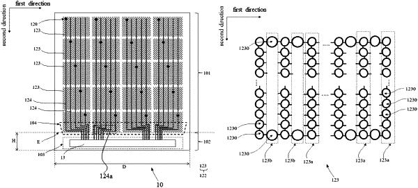
wherein the plurality of touch control sensing blocks comprise a plurality of touch control electrode lines;
wherein the plurality of touch control electrode lines of the plurality of touch control sensing blocks intersect to form a plurality of touch control line grids, and each of the plurality of touch control line grids corresponds to at least one of the sub-pixel units;
the plurality of touch control line grids comprise a plurality of first grid groups and a plurality of second grid groups, the plurality of first grid groups are arranged along a first direction and disposed at intervals, and at least one of the plurality of second grid groups is disposed between two adjacent first grid groups of the plurality of first grid groups; each of the plurality of first grid groups comprises a group of the plurality of touch control line grids arranged along a second direction and connected to each other in sequence, each of the plurality of second grid groups comprises another group of the plurality of touch control line grids arranged along the second direction, and the first direction intersects the second direction; and
a number of touch control line grids in each of the plurality of first grid groups is greater than a number of touch control line grids in each of the plurality of second grid groups, and the two adjacent first grid groups are electrically connected to each other by touch control line grids in the at least one of the plurality of second grid groups.
|