| CPC G06F 3/0418 (2013.01) [G06F 3/0412 (2013.01); G06F 3/04166 (2019.05); G06F 3/0443 (2019.05); G09G 3/3648 (2013.01); G02F 1/13338 (2013.01); G02F 1/136286 (2013.01); G02F 1/1368 (2013.01); G06F 2203/04107 (2013.01); G09G 2310/08 (2013.01); G09G 2320/0209 (2013.01); G09G 2354/00 (2013.01); G09G 2360/144 (2013.01)] | 18 Claims |
|
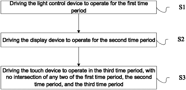
1. A display panel, wherein the display panel comprises a substrate, a light control device, a display device, and a touch device; the light control device, the display device, and the touch device are disposed on the substrate; the light control device, the display device, and the touch device are respectively operated in a first time period, a second time period, and a third time period, and any two of the first time period, the second time period, and the third time period are not intersected; wherein the light control device comprises a photosensitive thin film transistor and a switching thin film transistor electrically connected to each other, the display device comprises a display thin film transistor, and the touch device comprises a touch thin film transistor; and the photosensitive thin film transistor, the switching thin film transistor, the display thin film transistor, and the touch thin film transistor are disposed in a same layer and formed of a same material;
wherein the display panel further comprises:
a light control scan line electrically connected to the light control device so that the light control device operates in the first time period;
a display scan line electrically connected to the display device so that the display device operates in the second time period; and
a touch scan line electrically connected to the touch device so that the touch device operates in the third time period.
|