| CPC G06F 3/0416 (2013.01) [G06F 3/0481 (2013.01); G06F 3/04817 (2013.01); G06F 3/0482 (2013.01); G06F 3/0484 (2013.01); G06F 3/04883 (2013.01); G06F 3/04886 (2013.01); G06Q 10/10 (2013.01); H01L 29/24 (2013.01); H01L 29/42324 (2013.01); H01L 29/7827 (2013.01); H01L 29/78391 (2014.09); H01L 29/7889 (2013.01); H04L 65/403 (2013.01); H04N 21/47205 (2013.01); H04N 21/854 (2013.01); G06F 3/01 (2013.01); G06F 2203/04105 (2013.01); G06F 2203/04803 (2013.01); G06F 2203/04808 (2013.01); G11B 27/10 (2013.01); H04N 21/00 (2013.01); H04N 21/84 (2013.01)] | 14 Claims |

|
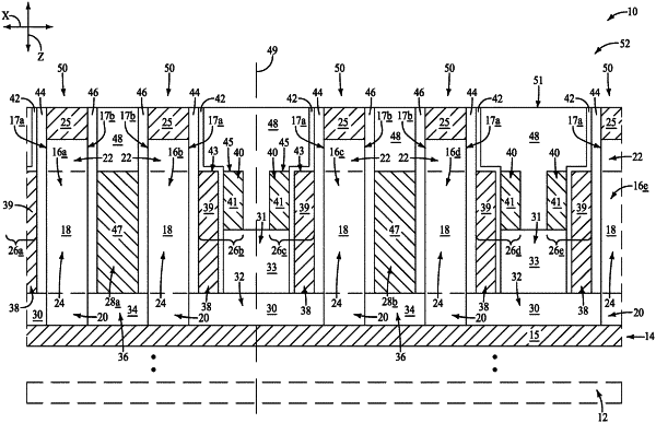
1. An integrated assembly, comprising:
a first comparative digit line;
pillars extending upwardly from the first comparative digit line, the pillars comprising semiconductor material; each of the pillars including, in ascending order, a first source/drain region, a channel region, and a second source/drain region; the first source/drain regions being coupled with the first comparative digit line;
a second comparative digit line coupled with the second source/drain regions; the first and second comparative digit lines being comparatively coupled to one another through sense-amplifier-circuitry;
each of the pillars having a first sidewall surface and an opposing second sidewall surface along a cross-section;
gating structures adjacent the first sidewall surfaces and vertically overlapping the channel regions; each of the gating structures including a first component which is electrically floating, a second component which is coupled with driver circuitry, and a ferroelectric material between the first and second components; and
conductive structures adjacent the second sidewall surfaces and vertically overlapping the channel regions, the conductive structures being configured to drain excess carrier from the channel regions and thereby alleviate floating body effects.
|