| CPC G06F 3/0412 (2013.01) [G06F 3/0418 (2013.01); G06F 3/04184 (2019.05); G06F 3/044 (2013.01); G06F 3/0443 (2019.05); G06F 3/0445 (2019.05); G06F 3/0446 (2019.05); G06F 2203/04111 (2013.01); G09G 3/3225 (2013.01)] | 7 Claims |

|
1. A display device comprising:
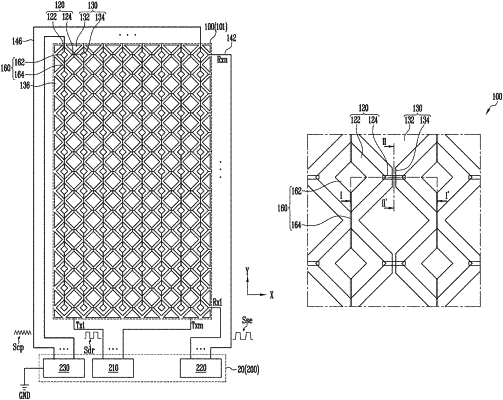
a display region, and a sensing region overlapping the display region;
pixels in the display region;
an encapsulation layer on the pixels;
sensing electrodes on the encapsulation layer, overlapping the sensing region, and comprising first electrode cells defining an opening, and first connection parts connecting the first electrode cells in a first direction;
driving electrodes on the encapsulation layer, overlapping the sensing region, and comprising second electrode cells that are spaced from the first electrode cells, and second connection parts connecting the second electrode cells in a second direction;
conductive patterns comprising electrode parts that are spaced from the first electrode cells in the opening of each of the first electrode cells, and connection lines respectively connecting two or more of the electrode parts;
a line connected to an end of the conductive patterns adjacent to an edge of the sensing region; and
a driving circuit configured to generate a noise compensation signal based on image data of each frame, and to supply the noise compensation signal to the conductive patterns through the line,
wherein the first connection parts or the second connection parts are at a same layer as the first electrode cells and the second electrode cells, and
wherein at least one of the first connection parts, the second connection parts, the first electrode cells, or the second electrode cells is directly on an upper surface of the encapsulation layer.
|