| CPC G06F 3/0412 (2013.01) [G06F 3/0443 (2019.05); G06F 3/0446 (2019.05); G06F 3/0448 (2019.05); H10K 50/84 (2023.02); H10K 59/122 (2023.02); H10K 59/40 (2023.02); G06F 2203/04111 (2013.01); G06F 2203/04112 (2013.01); H10K 59/12 (2023.02); H10K 59/351 (2023.02)] | 20 Claims |
|
1. An array substrate, comprising:
a base substrate, comprising a transparent display region and a non-transparent display region located at a side of the transparent display region, wherein the transparent display region comprises a plurality of anode regions and a transparent region;
a pixel drive layer, located at a side of the base substrate and at least located in the plurality of anode regions;
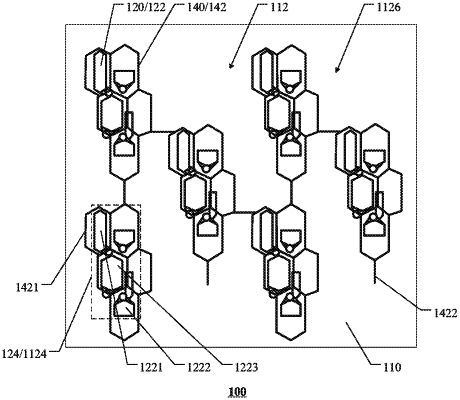
a plurality of anode groups, located at a side of the pixel drive layer away from the base substrate, and located in the plurality of anode regions, wherein each of the plurality of anode groups comprises a plurality of anodes, and the pixel drive layer is connected with the plurality of anodes;
a touch electrode layer, located at a side of the plurality of anode groups away from the base substrate and comprising a conductive mesh line,
wherein, in the transparent display region, an orthographic projection of at least partial conductive mesh line of the conductive mesh line on the base substrate winds along edges of orthographic projections of the plurality of anode groups on the base substrate.
|