US 12,079,145 B2
Distribution of data and memory timing parameters across memory modules based on memory access patterns
Max Ruttenberg, Bellevue, WA (US); Vendula Venkata Srikant Bharadwaj, Bellevue, WA (US); Yasuko Eckert, Bellevue, WA (US); Anthony Gutierrez, Bellevue, WA (US); and Mark H. Oskin, Bellevue, WA (US)
Assigned to Advanced Micro Devices, Inc., Santa Clara, CA (US)
Filed by ADVANCED MICRO DEVICES, INC., Santa Clara, CA (US)
Filed on Jan. 30, 2023, as Appl. No. 18/103,240.
Application 18/103,240 is a continuation of application No. 17/130,604, filed on Dec. 22, 2020, granted, now 11,586,563.
Prior Publication US 2023/0185742 A1, Jun. 15, 2023
Int. Cl. G06F 13/16 (2006.01); G11C 11/4076 (2006.01)
CPC G06F 13/1668 (2013.01) [G11C 11/4076 (2013.01)] 19 Claims
OG exemplary drawing
 
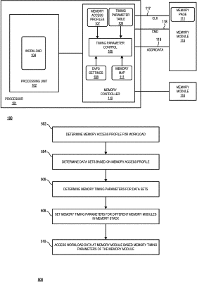
1. A method comprising:
identifying, for each of a plurality of memory modules, a corresponding memory access profile based on a workload to be executed at a processor; and
setting a memory timing parameter for each of the plurality of memory modules based on the corresponding memory access profile, wherein setting of the memory timing parameter for each of the plurality of memory modules is based on an expected pattern of memory access to data for executing the workload.