| CPC G05F 3/267 (2013.01) [G05F 1/461 (2013.01); G05F 1/468 (2013.01)] | 20 Claims |
|
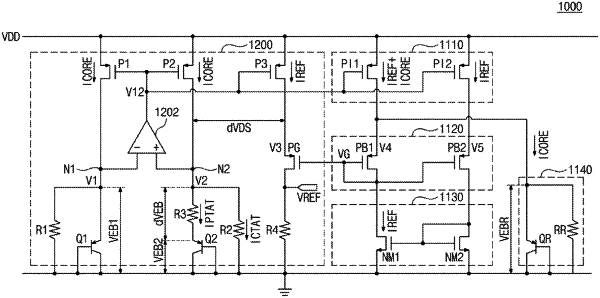
1. An electronic device, comprising:
a reference voltage generator circuit configured to generate a difference voltage and a reference voltage based on a first voltage of a first node and a second voltage of a second node; and
an adaptive cascode circuit configured to generate a bias voltage based on the difference voltage,
wherein the reference voltage generator circuit includes:
a first transistor including a gate to which the bias voltage is applied from the adaptive cascode circuit; and
a first current source configured to supply a first current to each of the first node and the second node and to supply a second current to the first transistor,
wherein the adaptive cascode circuit includes:
a second current source configured to output a third current and a replica current;
a voltage buffer configured to generate the bias voltage based on the third current;
a current mirror configured to mirror the third current; and
a replica circuit configured to be implemented as a replica of one or more components of the reference voltage generator circuit, and
wherein the voltage buffer includes:
a second transistor including a gate to which the bias voltage is applied and a second terminal to which the bias voltage is applied; and
a third transistor including a gate to which the bias voltage is applied.
|