| CPC G02F 1/13685 (2021.01) [G02F 1/136286 (2013.01)] | 11 Claims |

|
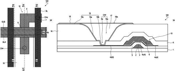
1. An active matrix substrate having a display region defined by a plurality of pixel regions arrayed in a matrix, the active matrix substrate comprising:
a substrate;
a pixel thin film transistor (TFT) supported by the substrate and located in a corresponding one of the plurality of pixel regions; and
a pixel electrode electrically coupled with the pixel TFT,
wherein the pixel TFT includes
a lower gate electrode provided on the substrate,
a lower gate insulating layer located so as to cover the lower gate electrode,
an oxide semiconductor layer provided on the lower gate insulating layer, the oxide semiconductor layer including a channel region opposing the lower gate electrode with the lower gate insulating layer interposed therebetween and a source contact region and a drain contact region located at opposite sides of the channel region,
an upper gate insulating layer provided on the channel region of the oxide semiconductor layer, and
an upper gate electrode provided on the upper gate insulating layer and opposing the channel region of the oxide semiconductor layer with the upper gate insulating layer interposed therebetween,
wherein the active matrix substrate includes
a lower gate metal layer that includes the lower gate electrode and a lower gate line electrically coupled with the lower gate electrode of the pixel TFT, and
an upper gate metal layer that includes the upper gate electrode and an upper gate line electrically coupled with the upper gate electrode of the pixel TFT, and
wherein a width of the upper gate line electrically coupled with the upper gate electrode of the pixel TFT is greater than a width of the lower gate line electrically coupled with the lower gate electrode of the pixel TFT.
|