| CPC G02F 1/1368 (2013.01) [G02F 1/13439 (2013.01); G02F 1/136277 (2013.01); G02F 1/136286 (2013.01); H01L 27/1225 (2013.01); H01L 27/1251 (2013.01); H01L 29/78648 (2013.01); G02F 1/13338 (2013.01); G02F 1/133388 (2021.01); G02F 1/13454 (2013.01); G02F 1/136295 (2021.01); G02F 1/13685 (2021.01)] | 14 Claims |
|
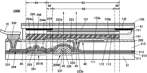
1. A display device comprising:
a display portion; and
a driver circuit portion,
wherein the display portion comprises a first transistor, a pixel electrode, a capacitor, a scan line, and a signal line,
wherein the driver circuit portion comprises a second transistor,
wherein the first transistor comprises:
a first gate electrode;
a first gate insulating layer over the first gate electrode;
a first semiconductor layer over the first gate insulating layer;
a first source electrode and a first drain electrode over and in contact with the first semiconductor layer;
a second gate insulating layer over the first source electrode and the first drain electrode; and
a first back gate electrode over the second gate insulating layer,
wherein the second transistor comprises:
a second back gate electrode;
the first gate insulating layer over the second back gate electrode;
a second semiconductor layer over the first gate insulating layer;
a third gate insulating layer over the second semiconductor layer;
a second gate electrode over the third gate insulating layer; and
a second source electrode and a second drain electrode electrically connected to the second semiconductor layer,
wherein each of the first semiconductor layer and the second semiconductor layer comprises a metal oxide,
wherein the scan line and the signal line each comprise a metal layer,
wherein the scan line has a region functioning as the first gate electrode,
wherein the signal line is electrically connected to one of the first source electrode and the first drain electrode,
wherein the other of the first source electrode and the first drain electrode is electrically connected to the pixel electrode,
wherein the pixel electrode, the capacitor, the first source electrode, and the first drain electrode each comprise a material transmitting visible light,
wherein the capacitor has a region overlapped with the pixel electrode, and
wherein the second gate electrode comprises an oxide conductor comprising an impurity element.
|